Bullstory Research July 7, 2026
Bottleneck at the inflection point of the AI agent
Key takeaways
KV cache creates a memory bottleneck, and 2026The commercialization of HBF in the year is the turning point that resolves it. HBF increases HBM capacity by 8~16fold, sharply boosting NAND demand. SK hynix is leading standardization.
The AI inference transition has turned NAND and SSDs from simple secondary storage into core resources for AI infrastructure. The storage needed for one AI server is 8~10 times that of a conventional server, so demand for enterprise SSDs for large-capacity, real-time access such as KV cache is surging. NAND demand is increasing by 20~22 percent annually, but as capacity shifts are slow, supply pressure continues.
1. The emergence of AGENT AI
AGENT AI is an AI that, when given a goal, independently makes a plan, chooses tools, executes them, and evaluates the results.
Existing LLMs were only chatbots. They were closer to a support role than to replacing humans.
However, AGENT AI comes directly into computers, works like a person, and carries out tasks.
And unlike LLMs, it makes money. To survive competition and monetize, AI companies are staking everything on AGENT AI models.
The AI bubble is still at an early stage. CAPEX investment cannot be reduced. Sunk costs will arise.
AGENT AI does far more work than LLMs, so countless bottlenecks emerge.
Power (SOFC, gas turbines) / CPU, GPU, TPU, NPU, HBM / memory DRAM, NAND, HDD / substrates, copper * interconnects such as optical communications
/power semiconductors, AI PCs / data center construction, neoclouds / bottlenecks are occurring countless times over.
2. Why AGENT AI now?
Traditional AI is a one-off chatbot that answers when you ask, and a person must give instructions every time.
AGENT AI judges and acts on its own through goal → planning → execution → feedback → repetition.
AGENT AI is a 24-hour automated digital worker that creates direct revenue by eliminating repetitive work, reducing labor costs, and increasing sales opportunities.
Exploding corporate demand "real cost reduction, sales increase"
-
Automation of repetitive work: Demand for AI employees across all areas, including support, sales, finance, and product
-
24 time AI staff: work progresses even when no one is present → increased revenue opportunities
-
Real cost reduction: among adopting companies, 83% removed repetitive tasks, 76% experienced productivity gains
Impact on profits: implementation cost < reduced labor costs + increased revenue → ROI (return on investment) is clear
3. Bottleneck in memory (DRAM·NAND)
KV CACHE: The main cause of the memory bottleneck
KV CACHE (Key-Value Cache) is a key cause of memory bottlenecks in the AGENT AI inference process.
What is KV CACHE? It is a technology that stores previously computed Key and Value values in memory when AI generates sentences, so they can be used immediately without being recalculated.
Problem: AGENT AI must process millions of tokens in real time, but if KV CACHE capacity exceeds the memory limit, the GPU has to just wait. This is the "Memory Wall".
Result: GPU compute speed has increased explosively, but if memory cannot supply data at that speed, expensive GPUs are wasted.
Background to the growing importance of NAND
With DRAM-based HBM alone, capacity limits (192GB) and cost burden are high.
NAND (NAND flash) is becoming important because:
-
Capacity: Compared with DRAM, 10 times more storage space
-
Cost: Compared with HBM, 8~16 times cheaper
-
Non-volatile: Data is retained even when power is cut
Key point: In the AI inference era, high-capacity, low-cost memory to hold the KV CACHE is essential → NAND demand explodes.
The structure by which the shift to AI inference is changing the NAND·SSD market (2024~2026)
With OpenAI’s o1 public (2024month, 9) as the turning point, the center of AI technology shifted from training to inference. This single structural shift changed the map of storage demand.
In the inference stage, models rapidly load large-scale data for each request. As access to KV cache and vector databases occurs continuously, demand for high-speed, high-capacity enterprise SSDs surged along with GPU demand (TrendForce, 2026month, 5).
The following is the visible change. 2026The storage required for one AI server in 8 to 10 times that of a conventional server. NAND demand increases by 20 to 22 percent annually, while supply only reaches 15 to 17 percent (Commercial Times, oscoo analysis, 2026). Demand is fast, but production and capacity conversion cannot keep up with that pace.
The paradox of shrinking NAND supply
The reason supply cannot keep up despite surging demand is the industry’s equipment allocation. Samsung and SK hynix are converting NAND lines toward HBM. That is because HBM margins exceed 60 percent. There are also reports that Samsung’s wafer output fell from 2025 units in 490 to 2026 units in 470. NAND capital expenditures rose only 5 percent year on year. Micron said its new fab will not be able to start operation until 2027. SK hynix said at its earnings release in 2025, 10 that year’s volume had already sold out (oscoo, storageswiss.com, 2026).2026.
This structural shift intensifies the short-term supply shortage. Demand is being reorganized around data centers and inference, while supply is moving toward high-margin HBM production. As a result, price and inventory pressure on enterprise SSDs increases.
SSD Prices and Market Changes — What Is Happening Now
Prices have already reacted. TLC 1terabit NAND unit prices went from 2025in the middle of the year 4.80dollars to 2025at the end of the year 10.70dollars, with a statement that they had doubled in 6months (Phison CEO, Tweaktown, 2025year 11month).
Consumer 1TB SSD prices also rose. Products that were **2025at the beginning of the year 45~60dollars rose to **2025after 9month of the year 70~90dollars or more. Sandisk disclosed a case in which it raised the price of the WD Black SN2026TB model at the beginning of the year from 8100 4dollars → 549.99dollars (Kingspec analysis, kitpa.org, 1,289.99year 2026month).2.
Micron decided in 2025month of the year 12to wind down its consumer brand, Crucial. It stopped shipping new consumer products from 2026month of the year 2and shifted all production to AI and enterprise use (oscoo, 2026year).
A Historic Shift as Enterprise SSDs Overtake Mobile
2026The year is likely to be the year when data centers first overtake mobile and become the largest source of NAND demand. The Sandisk CEO said at the 2026 earnings release in 1 that data-center NAND capacity growth would be in the "high single digits annually". Micron's 60 fiscal year NAND revenue is estimated by Wall Street to have risen by 2026% year on year to about 178billion dollars (Sandisk earnings release, Zacks, 236).2026}
TrendForce raised its outlook for the global NAND flash market size in 2026 to 2,706billion dollars. That corresponds to 281% growth year on year. TrendForce also projected further expansion to 2027billion dollars in 3,794. However, there is also an industry view that meaningful supply expansion will be difficult until around the 2027end of the year to 2028 or earlier (TrendForce, 2026 and 5).
Bottom line: As AI inference becomes the center of storage demand, NAND and SSDs have shifted from simple secondary storage to a core resource in AI infrastructure. Compared with the surge in demand, the conversion of manufacturing capacity is slow. For this reason, enterprise SSDs and large-capacity NAND have become short-term and structural investment points in the memory and storage sector.
HBF technology: breaking through HBM's capacity limit by 8 to 16 times
HBF (High Bandwidth Flash) is a next-generation memory that does not replace HBM, but complements HBM's capacity limitations.
Key explanation of HBF
-
Material: NAND flash (different from DRAM-based HBM)
-
Capacity: compared with HBM, 8~16 times larger (up to 4TB per GPU possible)
-
Speed: about 80~90% of HBM (fast enough)
-
Cost: at a similar cost, 8~16 times capacity
-
Role: HBM is cache (fast data processing), HBF is a library (storage for large-scale AI models)
HBF technical structure
-
3three-dimensional stacked NAND: multiple NAND dies vertically stacked into a single package
-
TSV (through-silicon via): vertically connects each NAND die, expanding bandwidth
-
CBA (wafer bonding): directly bonds memory cells and circuits, improving performance
-
multiple sub-arrays: maximizes read bandwidth through simultaneous access
Commercialization
-
2026 second half: first HBF memory samples provided
-
2027 early in the year: first sample of an AI inference device equipped with HBF
Related companies
-
SK Hynix: signed an MOU with SanDisk, leading HBF standardization
-
Samsung Electronics: produces both DRAM and NAND, holding an HBF opportunity
-
SanDisk (Western Digital): leading HBF technology development
Key point: 2026 commercialization of HBF in the year is a key variable in surging profitability in the memory market.
HDD demand surge: essential for large-scale storage
HDD (hard disk) is 5~8 times cheaper than SSD and optimal for large-capacity storage.
Background to the surge in HDD demand
-
AI data volume 3 times surged(2023~2028, 400zettabytes)
-
About 80% is stored on HDD for cost efficiency
-
Training and inference data archive: storage needed → HDD offers strong value for money
Recent HDD Market Trends
-
HDD price: supply price 4% increased, actual selling price 20% increased
-
HDD lead time: up to 1 years or more extended (shortage phenomenon)
-
2026 year: shipments rebounded
-
2028 year: shipments 2 units surpassed, single largest capacity 60TB reached
Related Companies
-
Western Digital: HDD world 1and above, immediately raising prices across all products
-
Seagate: HDD 2and above, announcing a plan to raise prices
Conclusion
KV CACHE is the key cause of memory bottlenecks, and **HBF is next-generation AI memory that 8~16breaks through HBM's capacity limits by a factor of
NAND is becoming increasingly important for its large capacity and low cost, and HDD is essential for large-capacity storage. (As SSD prices rise, HDD also benefits)
2026year HBF commercialization is a key variable for a sharp increase in profitability in the memory market. Led by SK Hynix, Samsung Electronics, and SanDisk.
4. Bottleneck in networking
AGENT AI does not work alone. Thousands of GPUs collaborate as a team to train or infer a single large model.
Problem: GPU processing speed has increased explosively, but the network speed connecting GPUs cannot keep up.
Result: GPUs spend more time waiting for data, causing expensive GPUs to be wasted. This is a "networking bottleneck".
If GPU connection speed cannot keep up with GPU processing speed, the entire AI infrastructure gets stuck.
Related Companies
-
CRDO: ultra-high-speed interconnect chip between AI accelerators Core: interface chip for data transfer between GPUs, before PAM4 high-speed transceiver
-
ALAB: CPO chip that integrates optical communications into the chip, GPU-to-GPU optical interconnect solution Core: first-mover advantage in CPO technology, leading integration of chip + optical modules
-
ANET: AI data center 400G/800G switches, high-bandwidth Ethernet switches Core: major customer of CLS, leading AI data center networking
-
CLS: high-bandwidth switches, white-box switches, core manufacturer of AI server rack and network switches (CPO-based switch manufacturing)
Background to the Spotlight on Optical Communications
Optical Communication is a technology that transmits data using light, and it is much faster than wires and consumes less power.
Why optical communication is drawing attention:
-
High speed: capable of transmitting several terabits per second (Tbps)
-
Low power: 50power savings compared with wires
-
Low latency: minimizes signal delay
-
High capacity: essential for massive data transmission in AI data centers
Key point: To connect thousands of GPUs in AI data centers, optical communications are essential.
Growth of MRVL
3Following a contract with Nvidia, it grew very sharply, and as it entered the Nvidia ecosystem, Jensen Huang recently 1made remarks about the company
-
Explosive growth in data transfer between AI servers → 800G·1.6T Ethernet switches demand surges
-
AI racks require optical communications → Marvell is a key supplier of optical transceivers
-
Along with Broadcom, Ethernet switch 2leader
-
Marvell is central to AI data center networks, a company that represents the networking and optical communications bottleneck in the substrate bottleneck structure
CPO technology: the key to solving networking bottlenecks
CPO (Co-Packaged Optics) is a technology that attaches optical communication components to a chip in a single package, reducing data transmission latency and power consumption at the same time.
Conventional method:
-
The optical communication module is separate from the chip
-
Data travels to the module over wires → power loss and latency occur
CPO method:
-
The optical communication module is in one package with the chip (physically integrated)
-
Data is directly connected → power 50% reduction, minimizing latency
CPO technology progress status
| Item | Details |
|---|---|
| Bandwidth | Existing 400G → 1.6T or more |
| Power | 50% reduction |
| Commercialization | 2026 years in full-scale adoption |
| Market | 2028 years 100 billion dollars or more |
Related companies
-
LITE : optical transceivers, lasers, detectors, and other core optical communications componentscore: supply of optical communication modules, production of optical devices for CPO support
-
COHR : high-performance optical transceivers: 800G/1.6T optical communication modules, lasers for optical communicationcore (high-bandwidth optical devices, supply of CPO optical modules)
-
AAOI : 400G/800G optical transceiver: for AI data centers, high-speed Ethernet solutionsCore: supply of optical communications modules, AI server networking
-
MXL : PPM: optical communications signal processing chips, analog components for networkingCore: optical communications signal processing, networking chips
-
TSEM : semiconductor packaging and chip integration, wafer bonding technology, 3three-dimensional IC packaging: technology for stacking chips vertically
-
VIAV : optical communications network testing and measurement, CPO test equipment
-
POET : optical interposer, Optical I/O: optical communications links between AI acceleratorsCore (securing leadership in CPO technology, chip + optical module integration)
-
KEYS : communications measurement equipment: optical transceiver performance verification, high-speed interface testing: 112G PAM4 check
-
GLW : Optical Fiber: ultra-fast interconnects between data centers, Glass Substrate: chip integration based on CPO
Photonic device materials: optical-communication components such as lasers and detectors core (optical-communication materials, supply of CPO glass substrates)
5. CPU bottleneck
The CPU bottleneck in the AGE AI era can be summed up as: “It is not enough for the GPU to be fast.” In agentic workloads, CPU-type tasks such as orchestration, memory management, data preprocessing, tool execution, and scheduling increase even more than inference itself, so the importance of the CPU has risen again.
Early generative AI seemed like “the GPU is everything,” but with AGE AI, the amount of work handled by the CPU has surged. AI agents do not just call the model; they have to coordinate multiple steps, call external tools, move data, and reconnect the results, so the CPU has taken on the role of traffic control for the system far more often.
The key point is that if the CPU is slow, the GPU ends up sitting idle. NVIDIA also introduced the Vera CPU and explained that agentic AI, reinforcement learning, data processing, and orchestration are CPU-intensive tasks, and that Vera is x86 faster than the CPU at completing agent tasks80%
Why is this a turning point now
The market already sees that the structure of CPU demand is changing. Some industry analyses said that in traditional LLM deployment, the CPU share was about 15%, but as AGENT AI spreads, that share could rise to 50%.
This change is not just a performance race; it also brings an architecture shift. Arm said that its share based on data center CPU revenue could jump to 2025in 50%, and there was also a forecast that in the AI ASIC server host CPU market, Arm-based CPUs could account for 2029at the beginning of 90%.
Related companies
-
AMD: In the period when CPU demand is rising again due to AGENT AI, AMD is increasing its share of server CPUs, and the EPYC lineup continues to take share from Intel
-
ARM: Hyperscalers that use Arm itself and Arm-based server CPUs are likely to benefit. Arm CPUs are highly power efficient, and in AI servers the role of the host CPU or traffic controller is becoming larger, so structural market share expansion is expected.
-
NVDA (Vera Rubin)
-
INTC
6. The arrival of Vera Rubin
Vera Rubin (Vera Rubin) is NVIDIA's next-generation AI platform, and it is not simply a faster chip, but a system that redesigned the entire AI factory from the ground up.
-
3.3 performance improvement: compared with Blackwell, 3.3 times performance, 3.5 times training, 5 times inference improvement
-
HBM4 installed: 6-generation high-bandwidth memory (exclusive supply from SK hynix and Samsung Electronics), 8 HBM4 stacks for ultra-high bandwidth
-
Vera CPU integration: a thoroughly AI-dedicated CPU that succeeds the existing Grace CPU, responsible for AI agents’ tool calls, code execution, and data processing
-
Rack-scale architecture: NVL72(72 CPU + 144 GPU) → one supercomputer
-
Power efficiency: compared with Blackwell, significantly lower compute cost per token
CPU market competition that Vera Rubin will bring
Vera Rubin signals NVIDIA’s direct entry into the CPU segment, and86creates a structural shift that adds NVIDIA to the competition of x (AMD and Intel) versus Arm.
Competitive landscape
-
NVIDIA vs AMD vs Intel: Vera CPU is designed exclusively for AI agents, reinforcement learning, and data processing; compared with existing x86 it delivers 50% faster performance and 2x efficiency
-
AMD share expansion: 2026 year 1 quarter x86 server CPU share rose to <strong>33.2%</strong>, while Intel 55% → declined
-
Rapid growth in Arm: Arm server CPUs achieved 2025 year 50%, and 2029 year 90% expected
Vera Rubin is a signal of a shift from GPU-centered AI infrastructure to CPU+GPU co-design.
NVIDIA's direct entry into the CPU arena while86x vs Arm vs NVIDIA3the semiconductor battle begins
Related companies
-
SK Hynix, Samsung Electronics, Micron : HBM4supply
-
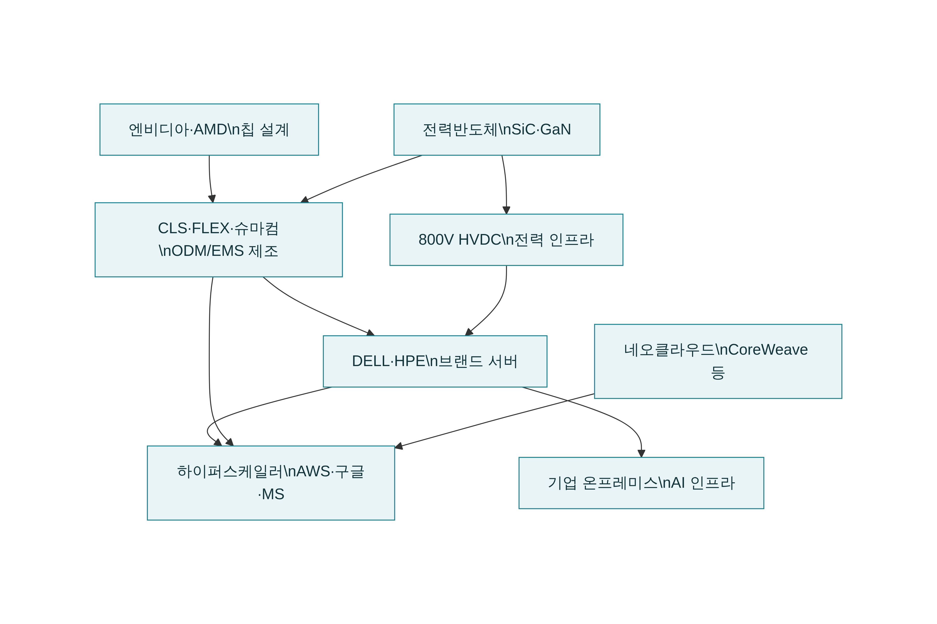
CLS : ODM manufacturing, AI server rack and network switch manufacturing, 1the above
-
FLEX : power management, cooling, 110kW power shelf, liquid cooling CDU supply
-
Hanmi Semiconductor : HBM packaging equipment
-
HPSP: server manufacturing, Vera Rubin NVL72 supported server supply
-
EO Technics: HBM4 test equipment
-
CRWV, NBIS: neocloud companies CoreWeave and Nebius are scheduled to adopt Vera Rubin (GTC 2026)
7. AI is moving beyond the cloud
AGENT AI is not just a simple response-type AI; it must judge and act in real time. That is why the limits of relying only on the cloud have become clear. The key reasons are latency, security, and cost.
Sending data to the cloud every time makes responses slower, sensitive information leaves the company, and usage fees rise as requests increase. So AI is increasingly moving closer to where the data is, where the devices are, and where the work happens.
On-premises AI
On-premises AI is a model in which a company runs AI directly on its own servers or inside its internal data center. It is especially important in places such as finance, healthcare, and the public sector, where data leakage would be critical.
The key is security and data sovereignty. Because data is not sent to an external cloud, compliance with regulations is easier, and sensitive data such as internal documents, customer information, and equipment data can be handled more safely.
Related companies
-
Dell, HPE: Representative infrastructure companies that build AI servers inside enterprises.
-
CLS, FLEX: Manufacturing partners behind DELL·HPE that produce actual servers, power, and networking equipment.
-
BiMatrix, Konan Technology, Synapsoft: Companies expected to benefit from domestic on-premises AI software and LLM demand.
On-device AI
On-device AI is a method of running AI directly inside devices such as smartphones, PCs, laptops, and cars. Because it does not go through the cloud, it is fast, works offline, and is advantageous for privacy protection.
The reason this approach has become important is that AGENT AI must respond immediately right next to the user. As personal devices such as AI PCs, AI smartphones, and wearables become the first execution space for AI, on-device AI is growing rapidly [http://있다.semiconductor.samsung).
Key beneficiary stocks
-
Apple, Samsung Electronics, LG Electronics: Representative companies that directly spread on-device AI in smartphones, PCs, and home appliances.http://기업들이다.blog)
-
Qualcomm: A key company in low-power AI computing chips and the NPU ecosystem
-
SK hynix, Samsung Electronics: Direct beneficiaries of growing demand for low-power memory for mobile and AI PCs.http://수혜주다.blog)
-
Openedges Technology, Chips&Media, Jeju Semiconductor: Often grouped as beneficiaries related to IP for on-device AI, video processing, and low-power memory.
Edge AI
Edge AI is a method of running AI directly at the site where data is generated, such as factories, cameras, robots, vehicles, and medical devices. The key point is that it makes an immediate judgment on site before sending data to the cloud.
The reason edge AI matters is real-time performance. Autonomous driving, industrial automation, smart cameras, and robots need reaction times in milliseconds, not seconds, so they cannot wait for a cloud round trip.
Key beneficiary stocks
-
NVIDIA: the center of the GPU and platform ecosystem for edge AI a company.
-
Qualcomm, MediaTek: key beneficiary stocks of demand for low-power edge AI chips
-
Samsung Electronics, SK hynix, Micron: representative beneficiary stocks as memory demand increases with the spread of edge AI.
-
LSCC, CEVA, SYNA: can be seen as beneficiary stocks for edge AI in terms of low-power FPGAs, design IP, and connectivity interfaces.
8. The importance of power semiconductors
Why has it become important?
AI servers are now more about how to deliver electricity stably, lose less of it, and reduce heat generation than about computation. NVIDIA also sees the existing 54V rack power architecture as unable to handle future MW-class AI racks, and is pushing a transition to 2027from 800V HVDC-based data center power infrastructure.
The key is power density. As GPUs increase in AI data centers, power loss, heat generation, and cooling burden all rise at the same time, and at that point power semiconductors that convert and control electricity become the bottleneck. That is why GaN and SiC power semiconductors, which are stronger than Si-based components in high voltage, high frequency, and high efficiency, have risen as core components.
Why SiC and GaN?
SiC is strong in high-voltage, high-temperature, and high-heat environments, making it advantageous for high-power conversion.
In practice, SiC is evaluated as reducing power loss and benefiting thermal management and system miniaturization because of its high breakdown voltage, high thermal conductivity, high operating frequency, and high operating temperature characteristics.
GaN is strong in higher switching frequencies and high power density. For AI data center 800V architectures, it is explained that GaN supports higher frequencies than SiC, making it suitable for high-density power supply structures.
800V HVDC: The Changes It Has Created
800The significance of the shift to V HVDC is not simply a rise in voltage. It is a structural change aimed simultaneously at improving power efficiency, reducing maintenance costs, and expanding power density.
The V HVDC architecture presented by Nvidia and Navitas showed effects of 800the existing 54V system versus improved power efficiency by up to 5percentage points, maintenance costs 70reduced by %.
This structural shift has elevated power semiconductors from “supporting components” to “core components of AI infrastructure.”
Some analysis also said that the GaN power semiconductor market is expected to grow at a compound annual rate of 2023 years 2hundred million7,100ten thousand dollars from 2030 years 43hundred million7,600ten thousand dollars, and 49%
Value Chain
In simple terms, the power semiconductor value chain has the structure of power supply → voltage conversion → rack distribution → internal server power conversion. Here, power semiconductors are used in UPS, PSU, DC-DC converters, and power modules, and their importance increases as AI servers become more power-intensive.
-
Device materials/chips: GaN, SiC power semiconductors
-
Power module/conversion: PSU, rectifier, DC-DC converter power+1
-
Power equipment: HVDC power supply devices, distribution systems, rack power infrastructure
-
End users: AI data centers, AI servers, MW-class racks
The reason power semiconductors have become important in the AI era is simple. It is more important to efficiently convert and withstand that electricity than to add more GPUs.
NVIDIA said it would shift from 2027since 800V HVDC-based AI data center power architecture, and GaN and SiC power semiconductors, which are strong in high-voltage, high-efficiency applications, have emerged as key components.
The most direct beneficiary is Navitas. In the global value chain, Infineon, ST, TI, and ROHM, and in Korea, power infrastructure companies such as LS Electric, HD Hyundai Electric, Hyosung Heavy Industries, and Sanil Electric can be seen as key beneficiaries.
Related companies
-
TXN: Official partner of NVIDIA
-
ON: NVIDIA official partner, the only vertically integrated SiC
-
NVTS: the only pure-play GaN
-
STM: Europe’s largest SiC + GaN
-
MPWR: DC-DC/IC
-
COHU: test equipment
-
AMKR / ASE: packaging
-
DB HiTek : Korea’s largest 8inch foundry
-
KEC : SiC 1200V localization
-
RFHIC : Korea’s only mass production of GaN
-
RF Materials : GaN RF packages, epi-wafer localization
-
QRT : specialized in reliability testing for power semiconductors, HBM testing
-
ALT : total solutions for back-end processing of non-memory chips
9. Server bottleneck — brand server companies vs. ODM/EMS
With the shift into the AGENT AI era, the bottleneck has moved to the entire server system.
When AI moves beyond the cloud, it is not enough to use just one data center; servers must be built separately in multiple locations.
As deployment sites are distributed from one cloud to thousands, tens of thousands, and hundreds of thousands of locations, overall server demand has grown exponentially.
Right now, securing one GPU is less important than timely supply of a server in which memory, power, cooling, boards, and network all work together so that the GPU can run properly **is more difficult.
In particular, AI servers have a much higher power density than conventional general-purpose servers, and their power delivery architecture is also more complex. As next-generation GPU power consumption has surged, the amount of power conversion and control components needed has structurally increased, and as a result, server assembly and delivery themselves have begun to become bottlenecks. In the market, it is believed that bottlenecks in components such as PCBs, power semiconductors, and cooling can even weigh on server growth rates.
What do branded server companies do
Branded server companies are, simply put, companies that design, integrate, and sell servers to customers. Representative examples include companies such as DELL and HPE.
They combine GPUs, CPUs, memory, storage, power equipment, cooling equipment, and networking into a single system and supply it to end customers. In other words, the face of the “finished server” that customers see is the branded server company.
What are ODM / EMS
ODM stands for Original Design Manufacturer, and it is a model in which the manufacturer handles both design and production. The company develops and manufactures products to meet the customer’s requirements, and then the branded company sells those products.
EMS stands for Electronics Manufacturing Services, and it refers to an electronics manufacturing services model that includes manufacturing, procurement, some design, testing, and logistics. Simply put, it is not just a simple assembly plant, but a manufacturing partner that runs the supply chain and production on behalf of the brand company.
The key difference is this. Brand server companies capture the market and customers, while ODM/EMS supports the actual product through design, production, procurement, and logistics.
In the AI server market, the two are less competitors than a symbiotic structure. Once a brand server company secures customers and defines server specifications, the ODM/EMS quickly turns that into a real product.
For example, brand companies such as DELL and HPE sell AI servers to enterprise customers and hyperscalers, but the chassis, boards, racks, power systems, and some network equipment inside them are designed, sourced, and produced by ODM/EMS partners such as Celestica and Flex. That is why, as AI server orders surge, not only brand companies but also ODM/EMS companies attract attention.
Why has ODM/EMS become more important?
In the AGENT AI era, servers have become a complex system that simultaneously incorporates high-density power, high-speed networks, liquid cooling, and advanced substrates rather than simple assemblies. In such a structure, it is difficult for brand companies alone to handle all manufacturing, and the value of ODM/EMS, which can move the supply chain quickly, increases.
In particular, Celestica is viewed as having a growth driver in its shift from traditional EMS to a high-value-added ODM model, and Flex is also expanding into a structure that goes beyond manufacturing to handle procurement, logistics, and power solutions.
Related companies
- HPE, DELL, SMIC, PENG, CLS, FLEX
10. Expanding the AI PC market
The biggest reason the AI PC market is growing is that AI is now changing from a tool that simply answers questions into a personal agent that runs right beside the user.
AGENT AI is not just for summarizing documents; it also needs to sort schedules, search files, summarize meetings, launch apps, and recommend tasks, so it has limits if it only round-trips through the cloud.
So AI has begun to move from the cloud into the PC. Running it directly on-device reduces latency, keeps personal information from going out as much, and lets some functions work even without the internet. In other words, the AI PC is the personal execution platform for the AGENT AI era.
In simple terms, an AI PC is a PC that includes an NPU as well as the CPU and GPU, so AI can run directly on the device. The key point is that generative AI functions can be handled locally in part without relying on the cloud.
Thanks to this structure, AI PCs handle functions such as meeting summaries, real-time translation, document organization, assistance with image generation, and personalized recommendations more quickly and naturally. Microsoft’s Copilot+ PC has become the representative benchmark for this market.
Share
AI PCs are now moving beyond a niche and into the mainstream. Based on Gartner, the share of AI PCs was forecast at <strong>2024year 15.6%, 2025year 31.0%, 2026year 54.7%</strong>, and the shipment volume in 2026year was presented at 1hundred million 4,311ten thousand units.
In the market, 2026there is a common view that AI PCs will exceed half of total PC sales in the year. ASUS also 2026AI PCs in the year will exceed 50percent of total sales, and 2027in the year they could go to 60percent or more.
NVIDIA, Microsoft, and Arm new AI PCs
The most important change is that NVIDIA has made a full-scale entry into the consumer PC market. NVIDIA, together with Microsoft, unveiled a new superchip called RTX Spark, presenting Windows PCs for the era of personal AI agents.
The core of this trend is Arm-based Windows AI PCs. Through Copilot+ PCs, Microsoft first established the standard for AI PCs, and the initial axis was Windows on Arm. With strong talk of NVIDIA also launching an Arm-based PC processor, the combination of Microsoft + NVIDIA + Arm has emerged as a new axis for next-generation AI PCs.
Related Companies
- ARM , NVDA, MSFT, DELL, ARM, QCOM
11. The Importance of NeoCloud
What is NeoCloud
NeoCloud is, simply put, an AI-only GPU cloud.http://모델이다.biz It is a model that focuses on GPU computing and AI workloads rather than a general-purpose structure like AWS or Azure that does everything, allowing faster supply.
Rather than replacing hyperscalers, they are closer to a complement that fills the gap in scarce GPU capacity. So the stronger the AI boom becomes, the more important NeoCloud becomes.
Why move to NeoCloud
Cloud market share is shifting from hyperscalers to NeoCloud.
The reason for moving from cloud to NeoCloud is that existing clouds have started to fall behind AI properly.
The key is GPU availability, latency, cost, and expertise 4to have.
1) GPU availability: existing cloud providers do not have enough GPUs
Driven by the surge in generative AI, demand for GPUs skyrocketed, but on existing hyperscalers it took 2~4 weeks, and in severe cases 3 months or more to secure GPUs.
About 3 out of 1 AI companies are facing delays in securing GPUs, and some companies have to wait 90 days. AGENT AI involves many inference calls and requires real-time responsiveness, so this kind of waiting time is enough to delay the project itself.
2) Latency: existing cloud providers are too slow
About 3 out of 1 enterprise AI users said that reducing latency was the main reason they chose NeoCloud.
Existing cloud providers are designed to handle general-purpose workloads such as web services, databases, and streaming, so using them exclusively for AI computation creates inefficiency and latency. By contrast, NeoCloud provides infrastructure optimized for AI computation, including GPU-centric architecture and high-speed networks (NVLink, InfiniBand).
3) Costs: Existing cloud is expensive
The share that cited cost as the main reason for using neocloud was 13% , but nearly half of them said they had switched from a major legacy cloud provider to neocloud and reduced costs by more than 25% .
The GPU instances of legacy hyperscalers were often criticized as a structure built on generic infrastructure, so using them for AI computation alone caused money to leak away. In fact, based on NVIDIA H100 DGX instances, neocloud hourly pricing was found to be about 66% cheaper than hyperscalers .
Also, neoclouds have fewer hidden costs related to data transfer and storage, making it much easier to predict total costs.
4) Expertise: Existing cloud is general-purpose, while neocloud is AI-specific
Neoclouds are a structure that has stripped away unnecessary elements. Designed to do a small number of things very well, they provide GPU capacity quickly and are optimized for AI workloads.
While traditional cloud is designed to handle general-purpose workloads, neoclouds natively come equipped with a GPU-centric architecture and an AI software stack. This gives them greater competitiveness than general cloud in advanced GPU-based AI workloads.
Related companies
CRWV
CoreWeave is currently the leading player in neoclouds. The market views CoreWeave as the largest neocloud operator, and assesses that it is growing rapidly on the basis of long-term contracts and a large backlog.http://평가한다.finance.yahoo)
The strength lies in the GPU cloud platform itself. Rather than simply leasing data centers, the core is a full-stack structure that provides managed GPU services and a software layer for AI workloads as well.
NBIS — Nebius
Nebius is one of the 2026by year-end, annual revenue run-rate to 70hundred million to 90billion dollars** .
It also won validation from hyperscalers by signing contracts with major customers such as Microsoft and Meta. With Nvidia’s investment added on top, market attention increased.
IREN
IREN originally started from a Bitcoin mining infrastructure base, but it is now transitioning into an AI cloud and HPC infrastructure company. The key point is that it already has power and land secured and is rapidly converting them into AI GPU infrastructure.seekingalpha+1
In particular, the 5-year contract with Microsoft drew the market’s attention. In the market, IREN is seen as a representative case of “turning power-based infrastructure into an AI cloud.”
APLD — Applied Digital
Applied Digital is a little different from other neoclouds. Rather than directly operating a cloud platform, it has strengths in liquid-cooling-based AI data center campuses and leased infrastructure there is.
In other words, APLD is less a “company that sells GPUs as a service” and more an infrastructure operator that builds and leases AI data centers. As AGENT AI grows, not only GPUs but also power, cooling, and the campuses themselves become scarce, so this kind of business also becomes important.
12. AI substrate bottleneck
The background for the substrate emerging as a bottleneck in AGENT AI is that, as AI not only boosts GPU performance but also processes “continuous large-scale inference” in real time, the technical difficulty and supply pressure on substrates surged at the same time.
| Cause | Explanation |
|---|---|
| Higher processing performance → surge in signal throughput | As the computing performance of AI semiconductors rises, more signals must be processed faster, so the difficulty of substrate technology rises sharply |
| Competition in advanced process nodes → expansion into packaging competition | As competition in semiconductor advanced process nodes expands into packaging competition, the existing CoWoS bottleneck shifts toward FC-BGA, ABF, and high-layer MLB |
| Real-time large-scale inference → nonlinear demand for substrates and components | Because AGENT AI involves many repeated calls, continued conversations, and multi-step planning, demand for GPUs, MLCCs, PCBs, and substrates does not rise in simple proportion but in multiples |
| Conflict between HBM substrates and production lines | As HBM substrates and small PCB (mSAP) production lines conflict, delivery times have lengthened from 6 weeks to 6 months, spreading supply-chain bottlenecks across the board |
| Certification period of 6+ months when changing suppliers | When changing suppliers for substrates and components, the certification period requires at least 6 months, so the bottleneck is highly likely to persist structurally |
| Slow expansion of packaging, underfill, testing, optical communication, and probe card capacity | The expansion pace of key component suppliers is slower, so bottlenecks are spreading across the board, and bottleneck segments are emerging as areas with pricing power |
| Broadcom points to constraints in the AI supply chain | Broadcom identifies TSMC advanced process technology, lasers, and PCBs for optical transceivers as key constraints, and the lead time for optical transceiver PCBs has lengthened from 6 weeks to 6 months |
AI servers have not only seen higher chip performance, but also simultaneous increases in package size, wiring density, power consumption, and network speed, which has sharply raised the specifications for substrates and components. As a result, bottlenecks are shifting in order from CoWoS packaging → ABF/FC-BGA → MLB/CCL → MLCC, and benefits are concentrating especially on companies that can handle high-layer, large-area, low-loss materials.
FC-BGA / ABF / glass substrate
-
FC-BGA: a high-density package substrate, a high-performance substrate that mounts semiconductor chips by flipping them over (Flip-Chip), connects GPUs, CPUs, and AI chips to the substrate, and handles high power and high signal processing
-
ABF substrate: the core insulating material of FC-BGA, a film material that creates the insulating layer in FC-BGA substrates, a key material that makes the high-layer structure of FC-BGA substrates possible, and high-performance FC-BGA cannot be produced without ABF
-
Glass substrate: solves the limits of organic substrates (ABF) in warpage, heat, and precision
The core background of the FC-BGA bottleneck is that, as AI GPUs and ASICs become larger, both substrate layer counts and area increase at the same time, while expansion at the high end cannot keep up with demand.2026Mirae Asset Securities analyzed that, with Hopper giving way to Blackwell, Rubin, and Feynman, FC-BGA demand and ABF layer counts will keep rising, and that server FC-BGA is likely to shift to a supplier-favored market thereafter.
FC-BGA: larger AI GPUs/ASICs, higher layer counts, limited expansion speed
ABF substrate: bottleneck shifts after CoWoS easing, surging demand for high-layer-count ABF
Related companies
-
Samsung Electro-Mechanics: a representative beneficiary with both FC-BGA and MLCC
-
Daeduck Electronics: FC-BGA for servers and semiconductors
-
LG Innotek: Expected ASP improvement from entry into FC-BGA for CPUs
Among U.S.-listed companies, packaging, assembly, and high-reliability substrates are more realistic than a pure ABF producer
-
AMKR: Benefit from the expansion of advanced packaging
-
SANM (Sanmina): Benefit from backplane and substrate assembly for AI server infrastructure
-
Glass substrates: SKC, Samsung Electro-Mechanics, Chemtronics / INTEL, GLW
PCB·MLB·CCL
-
PCB: printed circuit board, the basic board that connects multiple components in electronic devices
-
MLB: multilayer board, a board made by stacking PCB into multiple layers (usually 4 layers or more), and for AI servers, 18 layers or more of high-multilayer MLB are essential
-
CCL: copper-clad laminate, the base material used to make PCB, determining signal loss and voltage stability. For AI servers, M8→M9 series low-loss, high-performance CCL is needed, and bottlenecks arise due to supply constraints in low-CTE glass fiber and HVLP copper foil
The bottleneck in PCB and MLB comes from the rapid acceleration of AI servers, switches, and network equipment, which is driving demand for 18 layers or more of high-multilayer MLB sharply higher while also increasing process loads and yield difficulty. In particular, Mirae Asset Securities said that MLB with 18 layers or more will be the segment with the highest growth rate in 2024~2029 and explained that the expansion of multilayer stacking methods is key to ASP increases
The CCL bottleneck is an upstream material bottleneck for PCB. With the expansion of AI servers and 800G·1.6T networks, demand for high-end CCL with low dielectric constant and low loss characteristics (M8·M9 series) has structurally increased, and bottlenecks have emerged as supply constraints in raw materials such as low-CTE glass fiber and HVLP copper foil have also overlapped. In other words, as PCB becomes faster, the structure is one in which there is a shortage not of simple laminates but of a “supply chain that can absorb high-performance CCL”
Related companies
-
PCB substrates: SYMC, TLB, Korea Circuit, TTMI
-
MLB substrates: ISU Petasys, Daeduck Electronics
-
CCL: Doosan, Solus Advanced Materials, Lotte Energy Materials
**TTMI (TTM Technologies) is the only PCB substrate company that manufactures in the United States
MLCC
- MLCC: miniature capacitors (charge storage components) made by stacking ceramic layers, power stabilization + signal filtering + prevention of sudden voltage fluctuations
The MLCC bottleneck is directly linked to rising power consumption in AI servers. As the power consumption of GPUs and ASICs increases, the installed volume of high-reliability, ultra-high-capacity MLCCs rises nonlinearly, and even though utilization rates at leading companies are approaching 90~100%, Capex remains conservatively controlled, so supply cannot expand quickly. Therefore, MLCC should be viewed not as a simple auxiliary component, but as a power-stabilization bottleneck.
Related companies
-
Samsung Electro-Mechanics: PCB (FC-BGA) + MLCC dual-tailwind large cap, in NVIDIA's next-generation racks PCB +233%, MLCC +182% simultaneous surge
-
LG Innotek: simultaneous production of PCB + MLCC, dual tailwind
Next-generation packaging technology
- Limits of fine process nodes → performance expansion through packaging
-
As semiconductor process nodes (3nm, 2nm) approach their limits, the strategy of expanding performance and power efficiency through packaging is emerging as a key approach
-
Packaging technologies such as TSMC’s CoWoS (Chip on Wafer on Substrate) are becoming a core competitive advantage in AI semiconductors
- AI chip larger die sizes → fewer chips per wafer
-
Hopper 30 units → Blackwell 16 units → Rubin 6 units, and 12inch wafers 1 sharply reduce the number of pure chips per wafer
-
To package large-area chips efficiently, next-generation technologies such as CoWoS and FO-PLP (Fan-Out Panel Level Packaging) are essential
- HBM integration → increased packaging complexity
-
Because high-bandwidth memory (HBM) must be integrated into a single package with AI chips, the packaging stage acts as a supply-chain bottleneck
-
TSMC CoWoS CAPA cannot keep up with demand 2024~2025 so the packaging bottleneck intensifies
- Multi-chip integration → interposer and redistribution layer required
-
Because GPU, CPU, memory, and networking chips must be tied together in a single packaging structure, materials and processes such as silicon interposers, redistribution layers, and underfill are essential
-
As both conventional FC-BGA and silicon interposers are showing their limits at the same time, next-generation alternatives such as glass substrates are emerging
- Packaging bottleneck → substrate bottleneck shift
-
2026TSMC's aggressive expansion of CoWoS CAPA has eased the packaging bottleneck
-
However, the bottleneck has shifted to ABF·FC-BGA·high-layer-count MLB·high-performance CCL·MLCC
The core of AI semiconductor competition is now in packaging and substrates rather than the chip itself.
-
Easing of the CoWoS bottleneck → emergence of bottlenecks in FC-BGA·ABF·high-layer-count MLB·high-performance CML·MLCC
-
Next-generation packaging technologies (CoWoS, FO-PLP, glass substrates) are key to large-area chip·HBM integration
3DIC Recent News: The new bottleneck in AI semiconductors, advanced packaging (2026)
3DIC is a technology that stacks chips vertically and combines them into one package. The short distance between chips speeds data exchange and reduces power consumption. TSMC’s CoWoS and SoIC, Intel’s Foveros, and Samsung’s I-Cube are each company’s implementation methods. HBM is also a 3DIC method for stacking DRAM dies.
The market size is expanding rapidly. Mordor Intelligence said the 2.5D·3DIC market grew from 2025 to 112 billion 4,000 million dollars, and by 2026 it is expected to reach 148 billion 4,000 million dollars. It expects average annual growth of 2031% through 32, reaching 451 billion 9,000 million dollars. Demand exists, but supply cannot keep up. An analysis says Nvidia uses 60% of CoWoS capacity, and CoWoS lines have become a bottleneck.
TSMC said it would raise CoWoS production to monthly 2026wafer units by the end of 15, and it is putting a significant portion of its capital expenditure of 520 billion to 560 billion dollars into packaging. The problem is technical limits. The yield for 12-layer HBM3E remains in the low 50% range, and the yield of around 8~70% at 80 layers drops below 12% when moving to 50 layers, pushing package cost to almost double. Package power exceeds 1,400~2,000 watts in Blackwell- and Rubin-class chips, making it difficult to handle with existing cooling.
Design automation is still an unfinished area. Cadence released Millennium and Allegro X AI in 2026 and 4, but said final signoff remains the customer’s pain point. Moves to expand the ecosystem are clear. IC-Link under imec joined TSMC’s 3DFabric Alliance, and Intel unveiled its EMIB-T roadmap. Samsung is pursuing a design that seeks to bypass TSMC’s bottleneck with a turnkey strategy that combines foundry, memory, and packaging.
From an investor’s perspective, the key is simple. The pace at which the CoWoS bottleneck is resolved is a leading indicator for GPU shipments and HBM demand. 3DIC yields must rise for the high-cost structure to ease and AI server supply to accelerate. Samsung’s HBM4 and whether packaging turnkey orders are won are major variables for domestic semiconductor stock prices in 2026-2027.
Related companies
-
ASE: the world’s largest advanced packaging specialist, holding a CoWoS alternative technology that competes with TSMC’s CoWoS
-
AMKR: benefiting from the expansion of advanced packaging, benefiting from high-reliability packaging and assembly based in North America
Summary
It is clear that, at this turning point toward AGENT AI, numerous bottlenecks have emerged.
Now companies make money with AI, and within companies AGENT AI replaces people.
Big tech companies are aggressively increasing CAPEX spending, such as Google’s paid-in capital increase and Meta’s investment, and this investment cannot stop.
It would be good to find a better leader among the pick-and-shovel companies than among the mining companies and carry it forward as a leading stock.
While continuing to push the current leading sectors, optical communications and memory semiconductors, as the next bottleneck companies attract funds and / if they break out technically, I think it would be good to increase the position further.
Frequently asked questions
At the inflection point of AI agents, how does a shortage of GPU supply create bottlenecks for corporate profits?
A shortage of GPU supply limits computing capacity, raises costs, and slows product adoption and revenue expansion.
Why does KV cache become a bottleneck in AI agents?
KV cache processes millions of tokens in real time, exceeding memory capacity and leaving the GPU idle.
What impact does real-time inference latency have on AI agent product adoption, and how can it be reduced?
Real-time inference latency slows product adoption and reduces revenue opportunities. It is eased with large-capacity, low-cost memory (HBF, NAND), networking (optical communications, CPO), and cache optimization.
What is HBF, and what does it mean for the memory market?
HBF is NAND-based high-bandwidth flash that offsets HBM’s capacity limits by 8~16times. If commercialized, it becomes a factor that improves profitability through demand for large-capacity caches.
Between NAND and HDD, which is more important in AI infrastructure?
It depends on the use case. NAND is important for large-capacity, low-cost KV cache, while HDD is important for long-term storage of training and inference data.