Bullstory Research June 17, 2026
CPU? GPU? Now it's the era of the NPU!
Key takeaways
2026As of Year Month, the leading actor in on-device AI is the NPU. The NPU enables real-time inference with 6W-class ultra-low power consumption, allowing immediate application to smartphones, autonomous driving, and home appliances. Samsung Electronics is considered the biggest beneficiary in the foundry supply chain.1 types
In-Depth Report on the On-Device AI Value Chain Set to Dominate the Post-NVIDIA Era
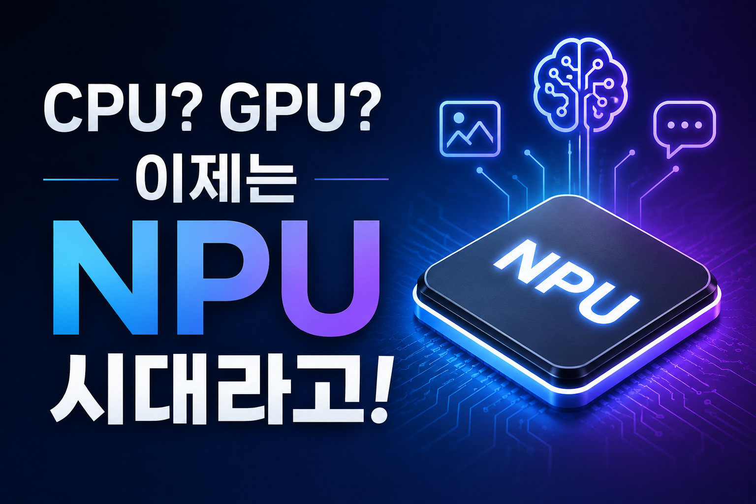
How long will you keep watching only NVIDIA GPUs and the HBM supply chain?
The CPU that began the history of semiconductor computers, the GPU that opened the spectacular prologue of artificial intelligence…
The next throne unquestionably belongs to the NPU (neural processing unit).
If you do not understand this trend, you will inevitably be completely left behind by the semiconductor megatrends 2026after the year onward.
The artificial intelligence (AI) infrastructure investment cycle that heated up global stock markets is entering a major period of qualitative transition. The pace of building “big tech data center infrastructure (GPU·HBM),” into which big tech companies had poured astronomical sums over the past several years, is gradually entering a period of stability.
The smart money of Yeouido and Wall Street is now moving rapidly toward the next stage of infrastructure development: the “On-Device AI” and “Edge AI” markets, where smartphones in our hands, on-device appliances, robots, and autonomous vehicles can think and make decisions for themselves without massive artificial intelligence servers.
The hardware that is the core brain cell of this enormous paradigm shift and that will hold absolute control over artificial intelligence computing is NPU (Neural Processing Unit)785. We will analyze the essence of the NPU ecosystem, which is changing the entire power map of design and distribution in the semiconductor industry, and thoroughly examine the key domestic value-chain beneficiary stocks whose order momentum has begun to be demonstrated in numbers in earnest, as of (2026 year 6 month).
1. The invisible wall of cloud AI: why on-device AI is inevitable
The AI based on large language models (LLMs) that has amazed the world until now was a perfect5520“centralized cloud”206 structure. When you ask an AI a question using a smartphone or PC, the data passes through a base station, travels along submarine fiber-optic cables, and is transmitted to a gigantic hyperscale data center. There, tens of thousands of densely packed NVIDIA GPU servers consume enormous amounts of electricity to perform the computations, after which they send the results back to our devices.
However, at a time when artificial intelligence must penetrate the tens of billions of devices in everyday life, this cloud-based approach faces three fatal limitations that make it unsustainable.
-
The limit of physical latency:
When a vehicle pursuing perfect autonomous driving detects an unexpected obstacle ahead, if data buffering of 0.2~0.3 seconds occurs while exchanging signals with a cloud server, this immediately leads to a major catastrophe. Robot control and remote medical surgery likewise depend on real-time responsiveness. -
The collapse of privacy and corporate security:
The fact that not only individuals’ sensitive biometric data and financial information, but also companies’ core confidential source code, is leaked to external servers every time for AI computation is the point of greatest concern for global regulators and companies. This is why secure “closed on-device computing” is being mandated against external hacking threats. -
Exponential server operating costs and global power shortages:
If people around the world use cloud AI dozens of times every day, the data center electricity costs and server maintenance expenses that Big Tech companies must bear will surge to levels that threaten their survival. Ultimately, the AI ecosystem can be sustained only by distributing the computational load to individual consumers’ devices (at the edge).
The only key that fundamentally solves these three chronic problems is on-device AI, which completes all AI inference inside the device itself without an external internet network connection774; the dedicated semiconductor created to implement this is the NPU.
2. Semiconductor Three Kingdoms: A Structural Comparison of CPUs vs. GPUs vs. NPUs
Why can’t on-device AI be implemented perfectly using existing CPUs or GPUs?
The answer becomes clear when we examine the architectural structure of semiconductors.
| Category | CPU (Central Processing Unit) | GPU (Graphics Processing Unit) | NPU (Neural Processing Unit) |
|---|---|---|---|
| Core structure | A few powerful cores (Sequential) | Thousands of general-purpose cores (Parallel) | Cores optimized for AI matrix operations (MAC-focused) |
| Processing method | Serial processing (complex instruction control) | Parallel processing (graphics pixel rendering) | High-speed matrix and vector operations (AI inference) |
| Power consumption | Typical | Very high (power hog) | Very low (ultra-low-power, high efficiency) |
| Form-factor constraints | Low | Very high (large cooler required) | Very low (easy to install in small devices) |
| AI efficiency | Low | High (suitable for training and large-scale inference) | Maximized (optimized for real-time inference on the device) |
CPU: The Cost of Serial Processing, Complex Instruction Control
The CPU, the brain of a computer, specializes in sequentially processing highly complex and varied instructions. Because it works like a structure in which a few brilliant geniuses solve problems one after another, it is structurally far too slow to process artificial-intelligence deep-learning computations in which hundreds of millions of simple matrix data points pour in at once.
GPU: The Powerhouse of Parallel Processing, the Origin of General-Purpose AI
The GPU that made NVIDIA the world’s leading company is a semiconductor originally created to use thousands of cores to draw monitor-screen 3D graphics pixels simultaneously. Its outstanding ability to process vast amounts of data at the same time—“parallel processing”—gives it excellent performance in AI training and large-scale computations. 하but because it is fundamentally a general-purpose chip designed for graphics, it contains processing units unnecessary for AI, consumes an enormous amount of power, and its large size means it cannot be installed in battery-powered mobile devices.
NPU: A Specialist Born Solely for Artificial Intelligence
An NPU is a specialized semiconductor designed to process at ultra-high speed while consuming as little power as 1W (watts), by using artificial neural network algorithms such as CNNs, RNNs, and Transformers that mimic the structure of neurons and synapses in the human brain. It boldly removes graphics processing and unnecessary general-purpose control circuits, concentrating solely on the matrix multiplication and accumulation (MAC) circuits at the core of AI inference.
As a result, when performing the same AI inference task, power consumption is reduced to 10th of that of a GPU while computational speed is overwhelmingly increased, achieving miraculous efficiency. This is the hardware-based reason why NPUs inevitably take the throne in smartphone, wearable, smart-home appliance, and automotive semiconductor markets, where power limits and heat control are essential to a product's survival.1:
3. From off-the-shelf clothing to bespoke tailoring: the great shift in semiconductor design power and the rise of DSP
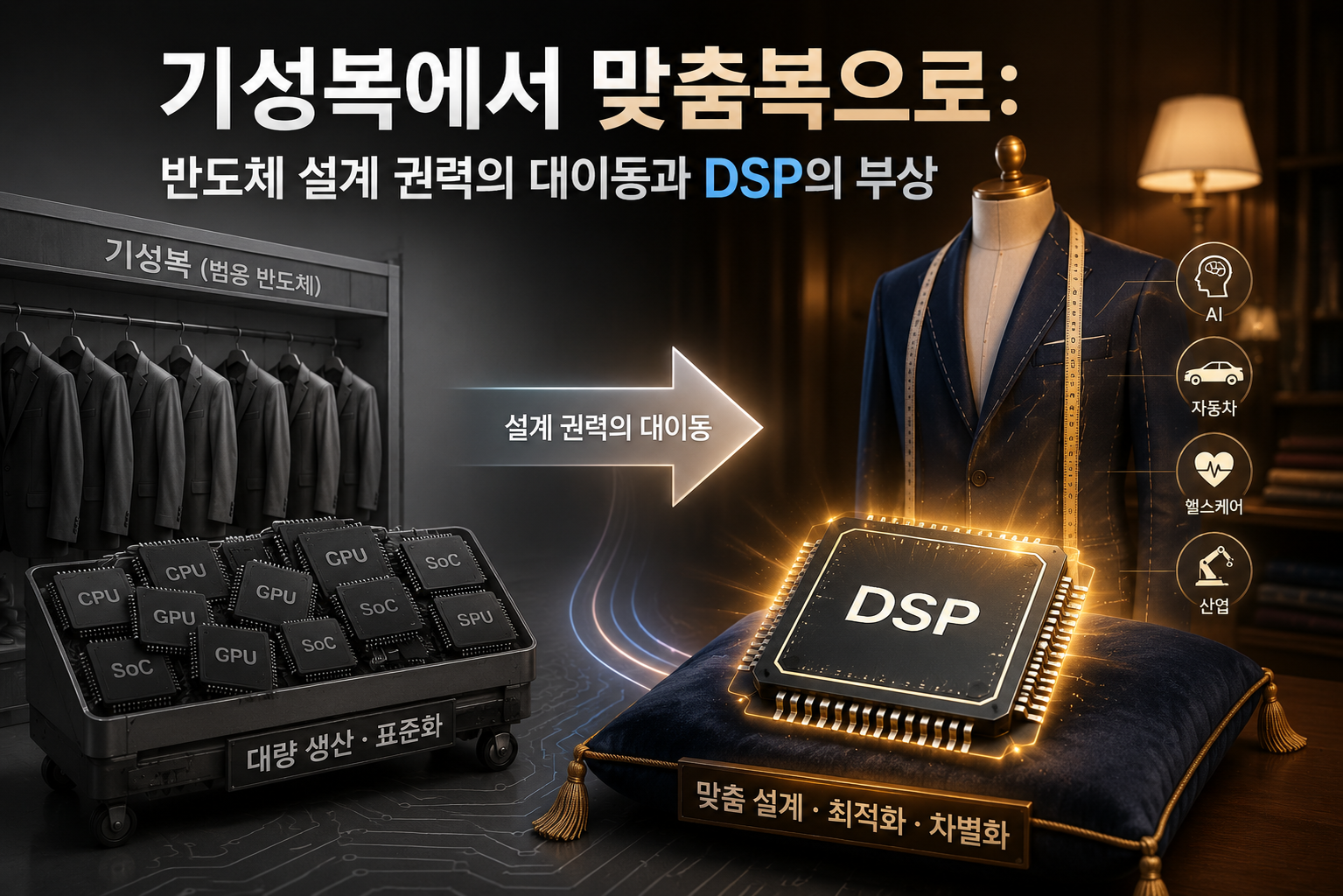
In the cloud AI market, it was enough to buy Nvidia's off-the-shelf general-purpose GPUs (H100, B200 and others) produced in mass quantities and install them in data centers. This is called the era of mass production of a limited range of products.
However, the on-device AI era is the era of perfectly customized, small-batch production (ASICs). The AI chip used in a smartphone, the AI chip used in a robot vacuum, the AI chip used in a smart refrigerator, and the AI chip installed in an autonomous vehicle must all have entirely different required computing capabilities (TOPS), permissible power consumption, and sensor interfaces.
Accordingly, global big tech companies (Apple, Google, Tesla, Meta, and others), as well as home appliance and automobile manufacturers, have begun directly designing their own customized NPU chips (application-specific semiconductors and ASICs) optimized by 100% for their product specifications, rather than using the general-purpose chips supplied by NVIDIA or Qualcomm as they are.
This is where a tremendous structural investment opportunity arises. Many companies around the world want to create their own NPUs, but implementing physical semiconductor circuit schematics to match fine foundry processes (3nm, 4nm, and so on) is an entirely different level of challenge. This is because it requires extremely costly fine-process assets and a skilled engineering infrastructure.
Ultimately, a new trickle-down ecosystem has emerged in which IP (intellectual property) companies that provide the core foundational semiconductor schematics, and design house (DSP) companies that convert fabless companies' abstract design schematics into final physical chips matching the specifications of foundries such as Samsung Electronics and TSMC, are monopolizing global custom NPU orders.
4. In the post-NVIDIA era, the TOP domestic NPU beneficiaries that must be included in your account 4
Amid the explosive growth of the global on-device AI market, particular attention should be paid to key domestic stocks that are absorbing exclusive custom NPU orders from global big tech companies while standing at the forefront of Samsung Electronics Foundry's advanced fine-process ecosystem. These are not merely theme stocks, but fundamentally driven stocks whose earnings are trending upward based on global order contracts.
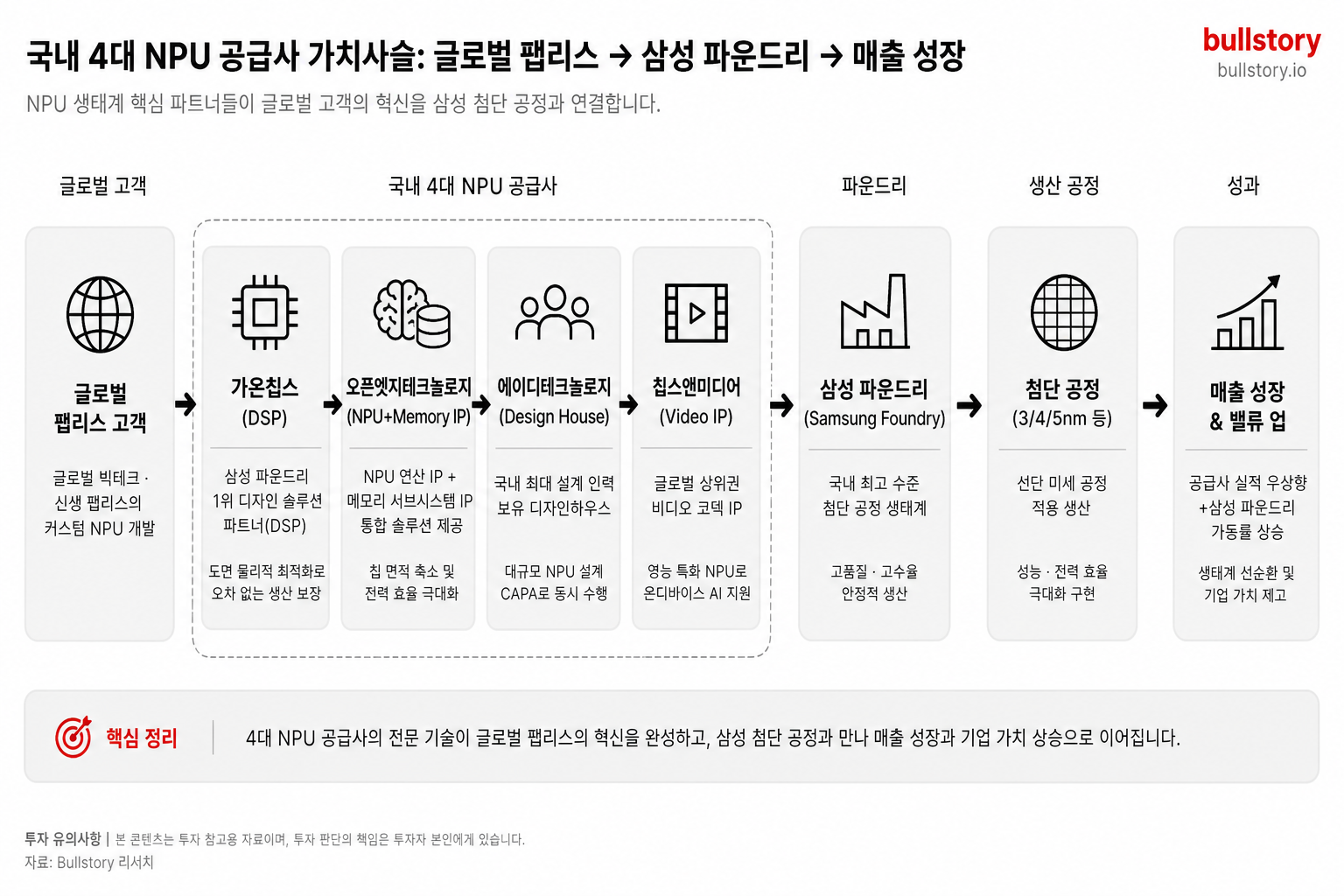
Diagram the value chain showing how four Korean NPU suppliers (DSP, IP, design house, video-IP) connect global fabless customers to Samsung advanced f
①Gaonchips (399720): The bridge for global advanced NPU orders and the undisputed leading DSP stock
Gaonchips performs the final physical optimization so that semiconductor designs created by global fabless companies and set makers can actually be manufactured without errors in Samsung Electronics' most advanced foundry processes (3nanometers, 4nanometers, 5nanometers, etc.) and is the overwhelmingly leading 1-tier Design Solution Partner (DSP) within the Samsung Foundry ecosystem.
-
Unrivaled high-value-added portfolio:
Gaonchips is not merely a low-priced legacy-chip company; projects involving automotive AI semiconductors, where technical barriers to entry are highest, and high-end on-device NPU chips account for a substantial portion of total revenue. It has the most extensive experience in fine-process chip design in Korea. -
Momentum from global territorial expansion:
After successfully establishing a subsidiary in Japan, a market that has recently been seeking a semiconductor revival, the company has successively won large-scale custom NPU development projects from major global customers in the region. Alongside rising utilization of Samsung Foundry's advanced processes, it is the undisputed leading stock in the sector, showing the clearest and most explosive earnings turnaround.
②Openedges Technology (394280): The world's only IP company that simultaneously opens up the brain and blood vessels of NPUs
It is a high-margin semiconductor IP specialist that does not manufacture semiconductors directly, but sells design assets (IP) that form the core foundation of chip design and receives licensing and royalty fees in return.
- Exclusive moat of the integrated AI platform:
OpenEdge's strongest technological barrier is that it is the only company in the world capable of providing 'NPU computing IP' and 'memory subsystem (PHY, controller) IP' as a fully integrated solution.
No matter how fast the NPU brain's computations are, if the high-speed memory highway carrying the data is blocked, the entire chip becomes paralyzed (a bottleneck). OpenEdge optimizes the high-speed organic connection through which data travels in one step, reducing chip area and maximizing power consumption, so it has established itself as an indispensable gateway for global emerging fabless companies seeking to develop their own on-device AI chips.\20;**85C;A stage is being reached in which a royalty-centered, high-profit structure becomes established.
③ (200710): A design house with overwhelming DSP leverage thanks to its large engineering scale
It is a design house company with a unique and substantial history, having shifted from being a key partner in the past TSMC ecosystem to becoming Samsung Electronics Foundry's official DSP.
- Scale advantage of design CAPA:
The core production capability of a design house business is none other than the number of skilled semiconductor design engineers785ADTechnology has the largest-scale design workforce infrastructure in South Korea. When global tech giants commission the small-batch production of various types of customized NPU chips worth trillions of won, it is one of the few companies in South Korea capable of completing multiple large-scale projects simultaneously without delays. Based on its close partnership with the global ARM ecosystem, it is a key market-leading stock whose share-price elasticity could surge just as strongly as Gaonchips when a large-scale spillover effect occurs.2.
④ Chips&Media (094360): The exclusive partner for all edge AI handling 'visual (video) data'
It is a unique company that has firmly maintained a top-tier global market share in the 'video codec semiconductor IP' field, which smartphones, automobiles, drones, and other devices must be equipped with to recognize objects.
- Transformation into a video-specialized NPU:
In line with the recent opening of the on-device AI market, it has successfully completed the development of its own 'video-dedicated NPU IP (NPU-VA)', perfectly specialized for real-time high-definition video data analysis, and has begun generating commercialization revenue. The areas where on-device AI is being deployed most disruptively are smart cars (ADAS), robotics, and AI CCTV, which must analyze real-time high-definition camera footage to enable autonomous driving and detect hazards. As its cross-selling strategy of embedding the new NPU IP into its network of hundreds of vehicle and IT semiconductor customers worldwide accelerates, it has entered a leverage phase in which revenue growth translates directly into net profit.
5. 2026Year second-half NPU sector investment strategy and key risk review
The NPU value chain is not a theme stock driven solely by expectations, but a 'structural broad-based upward cycle' arising from the shift in the central axis of the global supply chain785Therefore, rather than being swayed by short-term share-price fluctuations, a staggered buying approach from a medium- to long-term perspective is highly effective.
The Practical Investment Bible
-
Mid- to long-term portfolio diversification:
It is a reasonable strategy to make Gaonchips, which demonstrates the most stable earnings visibility as the sector leader, the solid central pillar of the portfolio (a beta play), and combine it with OPENEDGES Technology, which has boundless potential for technological royalty expansion, or Chips&Media, which has strong video-focused momentum, to maximize alpha returns. -
Thoroughly execute split-purchase entry points:
Even leading sectors with excellent companies inevitably experience temporary price adjustments due to global macroeconomic variables or foundry supply-and-demand issues. If the company’s unique moat has not been damaged, a strategy of actively increasing the allocation whenever the stock undergoes a beautiful pullback adjustment to the moving-average line or a major support level due to instability in overall market supply and demand is effective.60 days
Risk Factors That Must Be Checked
-
Advanced foundry yield and process-delay risks:
The earnings of design houses and IP companies are ultimately maximized when chips are successfully mass-produced at the foundry. If securing yields for cutting-edge fine processes at major foundries such as Samsung Electronics is delayed or big tech companies’ chip mass-production schedules are postponed, the timing of royalty and revenue recognition for related companies may be pushed back, so quarterly mass-production disclosures must be tracked closely. -
The pace at which global big tech companies internalize their own technology specifications:
A80;20;Hyperscale companies20;D514;If they succeed in building a fully self-developed in-house ecosystem without involving design houses or external IP at all, the order pool may shrink somewhat. However, as the number of small and medium-sized fabless companies is increasing explosively due to the nature of high-mix, low-volume production, the expansion of the overall market pie is structured to more than offset this.
6. Conclusion: Get ahead of paradigm shifts among market leaders
Historically, the stocks that have delivered the most enormous returns in the stock market have always emerged during the early stages when a 'new hardware standard' is established and deployed across the market. That was the case with component stocks in the early days of smartphone adoption, and with battery-materials stocks during the period of rising electric-vehicle penetration.
This is not the time to be consumed by chasing investments from behind, buying into the GPU and HBM rally centered on data centers after the fact. The on-device AI era, in which artificial intelligence emerges from the heavy iron gates of data centers to become the brain of every object in our daily lives, and the NPU value chain that serves as its heart, has just begun passing through the early stage of a massive, multiyear peak cycle.
Bet on the 'realm of knowledge and technology' that goes beyond hardware manufacturing to directly design and draw the blueprints for the customized brains of global big tech companies. **그**This will be the most certain and wise investment milestone running through the post-Nvidia era.
Frequently asked questions
What is the difference between a CPU, GPU, and NPU?
Key point: A CPU processes complex instructions sequentially, while a GPU handles large-scale computations with thousands of parallel cores. An NPU optimizes only matrix operations (MAC) to process real-time inference with low power consumption.
What is the difference between an NPU and a GPU?
Key point: GPUs are strong at general-purpose parallel computing, but consume substantial power and generate considerable heat. NPUs concentrate MAC circuits to reduce power consumption in the same inference to 10of the 1 level.
What is the structure of an NPU?
Key point: NPUs integrate large numbers of multiply–accumulate circuits (MACs) to perform matrix multiplication quickly. By removing general-purpose control, 1watt-class low-power designs are possible.
Which industries benefit from NPU-related stocks?
Key point: The beneficiaries are divided among fabless companies with NPU design, DSP, and IP; foundries and packaging; memory (HBM) suppliers; and embedded software companies.